This set of Microelectronics Multiple Choice Questions & Answers (MCQs) focuses on “Bipolar Cascode”.
1. What is the input impedance of the following circuit?
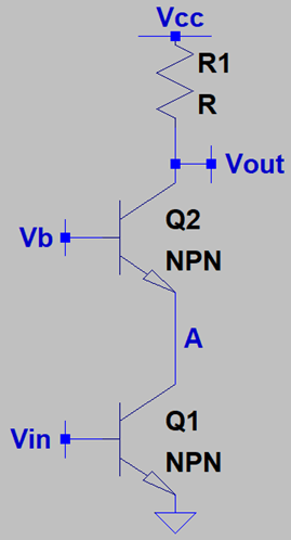
a) rπ1
b) rπ2 +rπ1
c) rπ2
d) Infinite
View Answer
Explanation: The input impedance of the circuit is simply rπ1. Q2 doesn’t impact on the impedance and only the impedance looking into the base of Q1 is the input impedance.
2. What is the input impedance of Q2?
a) rπ1 + (β+1) * ro2
b) rπ2 + (β+1) * ro1
c) Infinite
d) 0
View Answer
Explanation: Q2 is degenerated by the output impedance of Q1, looking into its collector, i.e. ro1. Henceforth, the input impedance becomes rπ2 + (β+1) * ro1. This is directly derivable from the expression of input impedance of a degenerated B.J.T.
3. What is the impedance looking into the collector of Q1 in the following circuit?
a) ro2
b) ro1+ro2
c) ro1
d) ro1+rπ1
View Answer
Explanation: The impedance looking into the collector of Q1 is independent of the rest of the circuit. This can be verified by a small signal analysis and hence, the impedance is ro1.
4. What is the impedance looking into the collector of Q2 in the following circuit?
a) (ro2+R1)*rπ2/(rπ1+(β+1)*rO2+R1)
b) (ro1+R1)*rπ1/(rπ2+(β+1)*rO1+R1)
c) (ro1+R1)*rπ2/(rπ1+(β+1)*rO2+R1)
d) (ro2+R1)*rπ2/(rπ2+(β+1)*rO2+R1)
View Answer
Explanation: We draw the small signal model of Q2 and readily note that VX=-Vπ and apply the Thevenin’s procedure of finding the resistance. Now, we apply a KCL at the collector node and find the current through ro. This current is gm*vπ+(IX-VX/rπ). Now, the current through RC is IX-VX/rπ. Finally, we apply a KVL from VIN, though ro and R1 to ground. After replacing the current and rearranging carefully, we reach the expression of impedance as (ro2+R1)*rπ2/(rπ2+(β+1)*ro2+R1). Note that we have calculated the input impedance of a CG stage with early effect.
5. What is the impedance at node A if all the transistors experience early effect?
a) (ro2+R1)*rπ2/(rπ1+(β+1)*rO1+R1)||ro1
b) (ro2+R1)*rπ2/(rπ2+(β+1)*rO2+R1)||ro1
c) (ro1+R1)*rπ1/(rπ2+(β+1)*rO1+R1)||ro2
d) (ro1+R1)*rπ1/(rπ2+(β+1)*rO2+R1)||ro2
View Answer
Explanation: At node A, we have two branches. One branch is connected to the emitter of Q2 which gives an impedance as (ro2+R1)*rπ2/(rπ2+(β+1)*rO2+R1). The other branch is connected to the collector of Q1 which gives a collector impedance of ro2. When calculating the impedance, we turn off all the independent voltage sources and apply a voltage at node A. Henceforth, we find that the resistances offered by these two branches appear in parallel and the overall impedance becomes (ro2+R1)*rπ2/(rπ2+(β+1)*rO2+R1)||ro1.
6. What is the output impedance of the following circuit?
a) (1+gm1*ro1)(ro2||rπ2)+ro1||R1
b) (1+gm12*ro1)(ro2||rπ1)+ro1||R1
c) (1+gm1*ro2)(ro1||rπ2)+ro2||R1
d) (1+gm2*ro2)(ro2||rπ1)+ro2||R1
View Answer
Explanation: The output impedance of this circuit can be calculated by using the small signal analysis. We find that Q2 is degenerated by the output impedance of Q1 – the impedance looking into the collector of Q1 becomes (1+gm2*ro2)(ro2||rπ1)+ro2. This impedance is parallel to R1 and the overall impedance becomes (1+gm2*ro2)(ro2||rπ1)+ro2||R1.
7. What is the transconductance of Q1?
a) gm1
b) gm2
c) gm1+gm2
d) 0
View Answer
Explanation: The transconductance of Q1 is only gm1. Given the transistor is not degenerated, the transconductance remains gm1.
8. What is the transconductance of Q2?
a) gm1
b) gm2/1+gm2*(ro1)
c) gm1+gm2
d) gm1/1+(1/rπ+gm1*(ro1))
View Answer
Explanation: The transconductance of a transistor reduces after it gets degenerated. The new transistor is gm1/1+(1/rπ+gm1*(degenerating resistance)). Therefore, for Q2, the new transconductance is gm1/1+(1/rπ+gm1*(ro1)). Note that option b is valid if the current gain is very high. Since it hasn’t been mentioned, we cannot take it as the correct answer.
9. What is the voltage gain from VIN to node A in presence of Early Effect in all the transistors?
a) -gm1*(ro2+R1)*rπ2/(rπ1+(β+1)*rO1+R1)||ro2
b) -gm2*(ro1+R1)*rπ1/(rπ2+(β+1)*rO1+R1)||ro2
c) -gm1*(ro2+R1)*rπ2/(rπ2+(β+1)*rO2+R1)||ro1
d) -gm2*(ro1+R1)*rπ1/(rπ2+(β+1)*rO2+R1)||ro1
View Answer
Explanation: The voltage gain from VIN to node A is due to Q1 behaving as a CS stage. The voltage gain of a CS stage is given by –(transconductance * (output impedance)). This impedance is given by the output impedance at node A. The output impedance is calculated as (ro2+R1)*rπ2/(rπ2+(β+1)*rO2+R1)||ro1. The overall gain is -gm1*(ro2+R1)*rπ2/(rπ2+(β+1)*rO2+R1)||ro1.
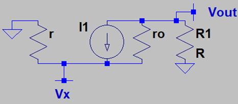
10. What is the voltage gain node A to VOUT in presence of early effect?
a) (1/ro1+gm1)(R1||ro1)
b) (1/ro2+gm2)(R1||ro2)
c) (1/ro1+gm2)(R1||ro1)
d) (1/ro2+gm1)(R1||ro2)
View Answer
Explanation: We draw the small signal model of Q2 & neglect Q1. Now, we calculate the current through ro2 as VIN-VOUT/ro2. Now, we write a KCL at the collector node and carefully rearrange the terms to get the voltage gain as (1/ro2+gm2)(R1||ro2).
11. What is the voltage gain for the following circuit in presence of early effect?
a) -gm1*(ro1+R1)*rπ1/(rπ1+(β+1)*rO1+R1)||ro1*(1/ro1+gm2)(R1||ro1)
b) -gm1*(ro2+R1)*rπ1/(rπ2+(β+1)*rO2+R1)||ro2*(1/ro2+gm1)(R1||ro1)
c) -gm1*(ro1+R1)*rπ2/(rπ1+(β+1)*rO1+R1)||ro2*(1/ro1+gm1)(R1||ro2)
d) -gm1*(ro2+R1)*rπ2/(rπ2+(β+1)*rO2+R1)||ro1*(1/ro2+gm2)(R1||ro2)
View Answer
Explanation: To calculate the voltage gain for the following circuit, we observe that VOUT/VIN=VOUT/VA*VA/VIN. Hence, we find that the overall voltage gain is the product of two voltage gain – one for Q1 behaving as a CS stage and one for Q2 behaving as a CG stage. For the CS stage, the gain is gm1*(ro2+R1)*rπ2/(rπ2+(β+1)*rO2+R1)||ro1 while that of the CG stage is ro1*(1/ro2+gm2)(R1||ro2). The overall voltage gain is the product of these two gains i.e. -gm1*(ro2+R1)*rπ2/(rπ2+(β+1)*rO2+R1)||ro1*(1/ro2+gm2)(R1||ro2).
12. What is the role of Q2 in the following circuit?
a) Cascode Device
b) Degenerating Device
c) Follower
d) Driver
View Answer
Explanation: Q2 is regarded as a Cascode Device. Q2 is regarded as the degenerating device. None of the devices behave as a follower or driver since Q2 behaves as a CG stage while Q1 behaves as a CS stage.
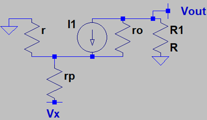
13. Suppose that a parasitic resistance appears in the emitter of Q2. What happens to the voltage gain of the following circuit?
a) 1/(1/((ro1+1/gm1)(R1||ro1))+rp/R1
b) 1/(1/((ro2+1/gm1)(R1||ro1))+rp/R1
c) 1/(1/((ro2+1/gm2)(R1||ro2))+rp/R1
d) 1/(1/((ro2+1/gm1)(R1||ro2))+rp/R1
View Answer
Explanation: We draw the small signal model of Q2 & neglect Q1. Firstly, we perform a KVL from VX to ground via rp & rπ. Next, we note that the current leaving the emitter node and goes toward the collector is VO/R1. Hence, we can now define Vπ in terms of Vin & Vout. Next, we perform a nodal analysis at the emitter node. Now, we note that the voltage gain from the emitter to VOUT is (ro2+1/gm2)(R1||ro2). Henceforth, we replace the nodal voltage in terms of VOUT & we can also replace Vπ. After carefully rearranging the terms, we will get the voltage gain as 1/ (1/((ro2+1/gm2)(R1||ro2))+rp/R1.
Sanfoundry Global Education & Learning Series – Microelectronics.
To practice all areas of Microelectronics, here is complete set of 1000+ Multiple Choice Questions and Answers.
If you find a mistake in question / option / answer, kindly take a screenshot and email to [email protected]
