Here are Microelectronics MCQs (Chapterwise).
1. Which effect is the bottleneck of speed in microelectronic systems?
a) Resistive
b) Power supply
c) Capacitive
d) Inductive
View Answer
Explanation: Capacitive effects get manifested in microelectronic devices which significantly limit the speed of such systems. The resistive effect leads to power dissipation while power supply would limit the effective working time and high-power applications.
2. Which of the following can be used to represent the input of a transconductance amplifier?
a) Thevenin’s equivalent
b) Norton’s equivalent
c) Schottky equivalent
d) Tellegen’s equivalent
View Answer
Explanation: The trans-resistance amplifier converts current to voltage. The input side should be represented by a Norton’s equivalent to represent the input current and the input impedance.
3. What is a Microprocessor?
a) Microelectronic Device
b) Digital system
c) Electrical system
d) Microelectronic system
View Answer
Explanation: It is not simply a digital system since it is prone to use microelectronic circuits and not simply logic gates. It would contain oscillators, filters and many other devices apart from the digital system. Microprocessors are kind of CPU which form a part of the Microelectronic System.
4. A D.C. voltage of 850mV is given to the base of a npn transistor, the reverse saturation current 5*10-17A while the emitter is grounded. The collector is attached to a 1KΩ resistor which connects to a 10V power supply. If VCE(sat) is 200mV, choose the maximum VBE to drive the device into saturation at room temperature.
a) 631mV
b) 635mV
c) 636mV
d) Data not given
View Answer
Explanation: The maximum VBE is 634.71mV. The collector current at saturation is derived as VCE=IC * RC and hence, it results to 2μA. Thereafter, we use the relation VBE=VT*ln(\(\frac {I_c}{I_s}\)) and we know VT is 26mV at room temperature.
5. Choose from the following where Microelectronics has invaded since its birth.
a) All household and military electronic systems
b) Only military electronic systems
c) All electronic systems
d) All systems
View Answer
Explanation: The presence of microelectronics systems has led to the digital revolution in the world. Ever since the advent of microchip technology, such systems have risen and play a dominant role in the present world. They are present from cameras to toothbrushes, mobile phones to computers, the military, satellite communication and many more areas and these areas have become hugely dependent on microelectronic systems for speed, power consumption and noise immunity.
6. What is the relation between the drift velocity of electrons (ve) and that of holes (vp)?
a) ve < vp
b) ve = vp
c) ve > vp
d) No relation exists
View Answer
Explanation: The drift of velocity of flow of electrons is greater than holes since the mobility of electrons is seen to be more than holes. The mobility of electrons is 1350 cm2/V.s while the mobility of holes is 480 cm2/V.s.
7. What is the key characteristic of a semi-conductor?
a) Filtering
b) Stability
c) Amplification
d) Barrier potential
View Answer
Explanation: The presence of a barrier potential is indicative of the fact that the semiconductor doesn’t always behave as a conductor and again as an insulator. It can switch from one characteristic to another.
8. In semiconductor devices, which of the following leads to propagation delay?
a) Finite switching time of transistor and Capacitive effects
b) Finite switching time of transistor
c) Inductive effects
d) Capacitive effects
View Answer
Explanation: The transistor in inverters exhibit a finite switching time to switch from one state to another. This is one of the causes of propagation delay in integrated circuits. Another cause is the charging and discharging effect of the capacitors present in the circuit. The total propagation delay is due to both of these bottlenecks.
9. If the top of the valence band and the bottom of the conduction band occur for the same momentum, which of the following event occurs?
a) Heat is absorbed during recombination
b) Heat is generated during recombination
c) Direct recombination takes place
d) Indirect recombination takes place
View Answer
Explanation: Since the top of the valence band and the bottom of the conduction band occur for the same momentum, electrons won’t have to change their momentum to fall into the valence band and direct recombination takes place.
10. What happens to the junction capacitance at zero bias if temperature increases?
a) It decreases
b) It increases
c) It increases linearly
d) It remains constant
View Answer
Explanation: The capacitance is inversely proportional to the square-root of the built-in-potential. The built-in-potential is directly proportional to the temperature. An increase in temperature would lead to a increase in built-in-potential which in turn would reduce the junction capacitance at 0 bias.
11. What should be the input impedance of an amplifier if it returns a voltage as an output?
a) Highly resistive
b) Infinite
c) Zero
d) Cannot be determined
View Answer
Explanation: The input impedance of an amplifier is independent of the quantity it returns as an output. Thus, we cannot determine the required input impedance until we know which quantity is to be sensed at the input of the transistor.
12. What kind of feedback is being used in the Self-bias circuit?
a) Negative feedback
b) Positive feedback
c) Neutral feedback
d) No feedback happens
View Answer
Explanation: Negative feedback is used to take the collector current and feed it into the base. The collector voltage decreases with an increase in the collector current. A reduction in the collector voltage will lead to decrease in the amount of current provided as a feedback to the base. Since the base current has reduced, the collector current gets reduced. The collector current is thus regulated by the feedback mechanism.
13. If the diode is made to work as a voltage-controlled capacitor, what happens to the capacitance with increase in the reverse bias?
a) Capacitance decreases
b) Capacitance increases
c) Depletion capacitance decreases
d) Diffusion capacitance increases
View Answer
Explanation: As the width of the space charge region increases, the capacitance decreases since the two plane of charge start shifting away from each other.
14. Which of the following properties are present in the I/V characteristics of a diode?
a) Shifts left with decrease in temperature
b) Independent of temperature
c) Shifts right with increase in temperature
d) Shifts left with increase in temperature
View Answer
Explanation: The I/V characteristics show the effect of increasing temperature in a PN Junction. If we increasing the temperature, the space charge width decreases and the threshold voltage decreases. This shifts the I/V characteristics leftwards.
15. Which co-efficient, present in the mathematical expression relating the collector current to the bias voltage, plays a dominant role in differentiating a npn form a pnp transistor?
a) Mobility
b) Diffusivity
c) Emitter width
d) Both diffusivity and mobility
View Answer
Explanation: Diffusion is responsible for the majority current flow through the base emitter junction. The value of diffusivity plays the dominant role.
16. What happens to the transconductance of a MOSFET if it’s width is multiplied by a factor of 4? Assume that the drain current is constant.
a) It increases by a factor of 4
b) It decreases by a factor of 6
c) It increases by a factor of 2
d) It decreases by a factor of 3
View Answer
Explanation: The transconductance is proportional to square root of the aspect ratio, for a constant drain current. The transconductance, gm, is given by √μnCOX(W/L)(ID). We readily observe that if the drain current is constant, the transconductance would increase by a factor of 2 when the width is multiplied by a factor of 4.
17. Which capacitance is neglected during modelling the MOSFET?
a) Source-bulk
b) Gate-bulk
c) Gate-drain
d) Source-drain
View Answer
Explanation: The source and drain are situated far apart from each other. They don’t share a junction and the capacitance between them is the mostly neglected.
18. What is the ratio of Voltage at node A to the input voltage in the Cascode stage?
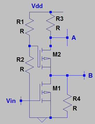
a) -gm2*(R4||ro1||(R1+ro2)/(1+(gmb2*ro2))
b) -gm1*(R3||ro2||(R1+ro2)/(1+(gmb2*ro2))
c) -gm1*(R4||ro1||(R3+ro2)/(1+(gm*ro2))
d) -gm2*(R3||ro2||(R3+ro2)/(1+(gmb2*ro2))
View Answer
Explanation: The ratio of the voltage at node B to the input voltage is the voltage gain of M1 being used as a CS stage. Hence, we can perform a small signal analysis and observe that the voltage gain is -gm1*the total impedance connected to its drain. This will be the output impedance at the node B. Node B has 3 branches. One branch connects to the source of M2 which offers an impedance of (R1+ro2)/(1+(gmb2*ro2) while another branch connects to the drain of M1 which offers a resistance of ro1. Finally, the last branch connects to R4 & all these resistances come in parallel. The overall output impedance is (R4||ro1||(R1+ro2)/(1+(gmb2*ro2)) and the voltage gain becomes -gm1*(R4||ro1||(R1+ro2)/(1+(gmb2*ro2)). Note that we can also calculate the voltage gain if M2 suffers from Body effect.
19. If the collector current through each transistor is 1.08mA, what should be the collector resistance so that the magnitude of the differential voltage gain is 8?
a) 266.66 Ω
b) 260 Ω
c) 250 Ω
d) 300 Ω
View Answer
Explanation: The magnitude of the differential voltage gain is the product of the collector resistance and the transconductance of the device, which is .03S in this case. The collector resistance should be not less than 266.66Ω. Note that both the resistors & the transistors are assumed to be equal.
20. If the impulse response of a system is sinc(t) and the laplace transform of the input is a pulse function ranging from -π to π, what will be the output?
a) sin t
b) sinc(t)
c) cos t
d) Unstable
View Answer
Explanation: The laplace transform of the impulse response is also a pulse ranging from -π to π. We note that the convolution in time domain is multiplication in s domain and hence, the Laplace transform of the output will also be a pulse ranging from -π to π. Finally, we take the inverse laplace transform to get sinc(T).
21. What is the -3db pole frequency of the following circuit? Assume that the OPAMP has a finite gain.
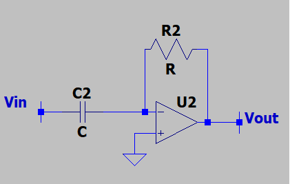
a) (G0)/R1C1
b) (G0-1)/R1C1
c) (1/G0+1)/R1C1
d) (G0+1)/R1C1
View Answer
Explanation: If the OPAMP has a finite gain, the voltage gain is -R1C1s/(1/G0*(1+R1C1s)+1). The 3db pole frequency is where the voltage gain drops approximately to √2 times the original gain. Hence, the pole frequency is (G0+1)/R1C1.
Chapterwise Multiple Choice Questions on Microelectronics

- Microelectronics Basics
- Basic Physics of Semiconductors
- Diode Models and Circuits
- Physics of Bipolar Transistors
- Bipolar Amplifiers
- Physics of MOS Transistors
- MOS Amplifiers
- Cascode Stages
- Current Mirror
- Differential Amplifiers
- Frequency Response
- Operational Amplifier
1. MCQ on Microelectronics Basics
The section contains multiple choice questions and answers on microelectronics basics.
|
|
|
2. Basic Physics of Semiconductors
The section contains questions and answers on the basic physics of semiconductors, properties of semiconductor materials, and semiconductor PN junctions, including breakdown characteristics.
|
|
|
3. Diode Models and Circuits
The section contains MCQs on the analysis of a PN junction as a diode, I/V characteristics of a diode, and applications of a diode.
|
|
|
4. Physics of Bipolar Transistors
The section contains Microelectronics multiple choice questions and answers on on the physics of bipolar transistors, characteristics of a BJT, modes of a BJT, and models of a BJT.
|
|
|
5. Microelectronics Questions on Bipolar Amplifiers
The section contains questions and answers on characteristics of bipolar amplifiers, Q-point analysis, and comparison of biasing methods, covering common emitter, common base, and common collector stages.
6. Physics of MOS Transistors
The section contains MCQs on on the behavior of a MOSFET and models of a MOSFET, offering a comprehensive understanding of MOSFET operation.
|
|
|
7. MOS Amplifiers
The section contains multiple choice questions and answers on common source stage, common gate stage, and common drain stage.
|
|
|
8. Microelectronics MCQ on Cascode Stages
The section contains questions and answers on MOS cascode and bipolar cascode.
|
|
|
9. Current Mirror
The section contains MCQs on MOS current mirror and bipolar current mirror.
|
|
|
10. Differential Amplifiers
The section contains Microelectronics multiple choice questions and answers on bipolar differential amplifiers.
|
|
|
11. Frequency Response
The section contains questions and answers on basics of frequency response, high frequency model of BJT and MOSFET, and low frequency response of stages of BJT.
|
|
|
12. Operational Amplifier
The section contains multiple choice questions and answers on opamp linear operations.
|
|
|
Wish you the best in your endeavor to learn and master Microelectronics!
If you find a mistake in question / option / answer, kindly take a screenshot and email to [email protected]
