This set of Power Electronics Multiple Choice Questions & Answers (MCQs) focuses on “Diodes Circuits-2”.
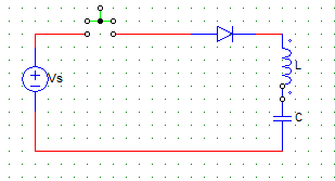
1. For the initially relaxed circuit shown below, KVL with switch in the closed position gives a certain equation. The Laplace of this equation will have the right hand side (RHS) as
a) Vs
b) (Vs x s)/RC
c) Vs/s
d) RC/s
View Answer
Explanation: When switch is closed,
Ldi/dt + 1/C ∫ idt = Vs
Laplace of the above gives,
L[sI(s)] + 1/C [I(s)/s] = Vs/s.
2. For the initially relaxed circuit shown below, the Laplace transform of the KVL when the switch is closed is
I(s) [ X ] = Vs/s
The value of X is
a) sL + 1/C
b) Cs + 1/sL
c) sL + 1/sC
d) Vs/CLs
View Answer
Explanation: When switch is closed,
Ldi/dt + 1/C ∫ idt = Vs
Laplace of the above gives,
L[sI(s)] + 1/C [I(s)/s] = Vs/s.
3. For the initially relaxed circuit shown below, if Ω=1/√LC. Then the current is a function of ___
a) cos Ωt
b) sin Ωt
c) tan Ωt
d) cos Ωt.sin Ωt
View Answer
Explanation: When switch is closed,
Ldi/dt + 1/C ∫ idt = Vs
Laplace of the above gives,
L[sI(s)] + 1/C [I(s)/s] = Vs/s
I(s) = Vs/(LΩ) * (Ω/Ω2 + s2)
Taking the inverse lapace gives,
I(t) = Vs * √ (L/C) * sin Ωt.
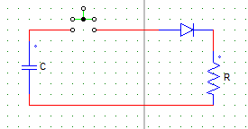
4. For the circuit shown below, the capacitor is initially charged to a voltage of Vo with the upper plate positive. After the switch (shown in green) is closed, the current through the load
a) increases from zero to Vo/R
b) decreases from Vo/R to zero
c) increases from zero to Vo/C
d) decreases from Vo/C to zero
View Answer
Explanation: The capacitor acts as a source. At instant switch is closed the current is maximum and than discharges till zero value through the load R.
5. For the circuit shown below, the capacitor is initially charged to a voltage of Vo with the upper plate positive. Switch is closed at t=0. The peak value of the current through the diode is
a) Vo/C
b) Vo/R
c) Vo
d) Vo/(RC)
View Answer
Explanation: When switch is closed, the equation is
Ri + 1/C ∫idt = 0 (Voltage across capacitor cannot change instantaneously)
Solution of the above equation gives, Vo/R at t= 0.
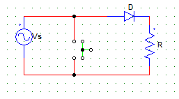
6. When the switch (shown in green) is closed, the average current through the diode in the positive cycle is
a) 0
b) Vs/R
c) Vs/(R+Rd)
d) none of the mentioned
View Answer
Explanation: The switch S.C’s the source.
7. When the switch is closed, the steady state current through the diode is
a) Vo/C
b) Vo/R
c) Vo
d) Vo/(RC)
View Answer
Explanation: I = Vo/R
8. When the switch is open, the current through the diode in the positive cycle is
a) zero
b) Vs/R
c) Vs/(R+Rd)
d) none of the mentioned
View Answer
Explanation: When the switch is open, the diode is forward biased and I = Vs/(Rd + R). Where, Rd is the diode resistance.
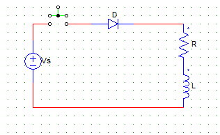
9. For the circuit shown in the figure below, consider the diode as an ideal diode & R.M.S value of source voltage as Vs.
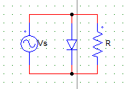
The output voltage waveform at R is most likely to have
a) zero value in the positive half cycle and a peak value of 1.414Vs in the negative half cycle
b) sine-wave nature with a peak value 1.414Vs
c) zero value in the negative half cycle and a peak value of 1.414Vs in the positive half cycle
d) sine-wave nature with a peak value Vs
View Answer
Explanation: The diode S.C’s the load in the positive half cycle.
10. For the circuit shown in the figure below, V8 is AC voltage source with peak value Vm. The waveform of the load voltage at the resistor is
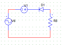
a) zero in the positive half & peak value of –(Vm) negative half
b) zero in the negative half & peak value of –(Vm-V1) in the positive half
c) zero in the positive half & peak value of –(Vm+V1) negative half
d) zero in the positive half & peak value of –(Vm-V1) negative half
View Answer
Explanation: Diode is reversed biased in the positive half cycle. In the negative half cycle, apply KVL to get the value of peak voltage at the load.
Sanfoundry Global Education & Learning Series – Power Electronics.
To practice all areas of Power Electronics, here is complete set of 1000+ Multiple Choice Questions and Answers.
If you find a mistake in question / option / answer, kindly take a screenshot and email to [email protected]
