This set of Basic Electronics Engineering Multiple Choice Questions & Answers (MCQs) focuses on “Junction Diode – Forward and Reverse Bias Conditions”.
1. What type of device is a diode?
a) Unidirectional
b) Bidirectional
c) Isolated
d) inappropriate
View Answer
Explanation: Diode is a device which allows current to flow only in one direction with ease. In the opposite direction, it far more difficult to conduct current for the diode. So, it can’t be acknowledged as a bidirectional device as that changes the properties and characteristics of diode. Hence, Diode is a unidirectional device.
2. Which region of the diode, does the anode corresponds to?
a) N-type
b) P-type
c) Depletion layer
d) Hidden
View Answer
Explanation: When the diode is biased by an external source, the anode is connected to the positive terminal and cathode to the negative terminal. P-type material has majority carriers as holes. If a potential difference is applied externally, the electrons in N-type would flow in a direction N-P i.e. cathode to anode and the direction of current would be from anode to cathode.
3. What is the voltage required across the P-N junction, to make it conduct in forward bias state for a silicon diode?
a) 0.3 V
b) 0.9 V
c) 0.7 V
d) 1.2 V
View Answer
Explanation: The forward biasing voltage is the voltage, which is applied across the P-N junction externally to make flow of current with ease. In forward biased state the anode is connected to positive terminal and cathode to the negative terminal of the external supply. Such voltage for Silicon diode is 0.7 Volts and for Germanium is 0.3 Volts.
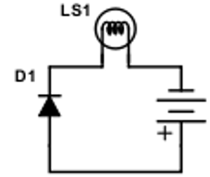
4. If the voltage across the Diode is 0.7 Volts and the rating of battery is 7 Volts, 1 Ampere then, what will the bulb do?
a) Defuse
b) Remain off
c) Partially glow
d) Glow
View Answer
Explanation: As seen in the figure, it is clear that the diode is forward biased and the voltage across the diode is 0.7 Volts, which the forward biasing voltage, due to which the current will flow and the bulb will glow. But, if the diode was reverse biased then even if we apply 0.7 volts the bulb would not have glowed.
5. When voltage is applied across cathode to anode then it is said to be ________ biased.
a) Reverse
b) Forward
c) Cyclic
d) Backward
View Answer
Explanation: When we apply a voltage across a reversed diode i.e. we are applying from cathode to anode (N-type to P-type). The diode is said to be reverse biased in this state, in which, it can resist current up to a certain limit depending on the physical conditions.
6. Name the maximum voltage that the diode can withstand, when a reverse bias voltage is applied to it.
a) Peak Voltage
b) Minimal Voltage
c) Peak Inverse Voltage
d) Minimal Inverse Voltage
View Answer
Explanation: When a reverse bias voltage is applied to a diode that means, we will connect the anode to negative point and cathode to positive point of an external potential difference. It can only withstand a voltage up to a certain limit. If the limit is crossed it undergoes breakdown called as Reverse voltage breakdown and that value is the Peak Inverse Voltage.
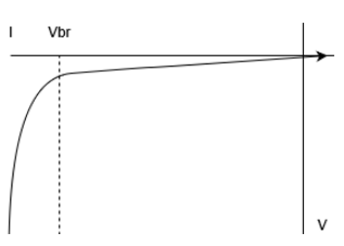
7. Which state of the graph shows the I-V characteristics of the diode?
a) Forward biased
b) Peak Voltage
c) Conducting state
d) Reverse Biased
View Answer
Explanation: As seen the graph we can observe that the values of current and voltage are negative. It clearly describes about the reverse bias state of diode, as it also shows the reverse breakdown and the Peak Inverse Voltage. The immediate declination of voltage after a point, is the breakdown.
8. How is the depletion layer in forward biased state as compared to reverse biased state?
a) Thin
b) Thick
c) Absent
d) Maximum
View Answer
Explanation: When the diode is forward biased, the electron from the N-type move to P-type much quicker than when they are in natural state. The external potential difference applied allows the diode to get to equilibrium sooner and also reduces the potential barrier. This creates an easy path for the flow of current, which make the depletion layer thin.
9. How is the resistance in the reversed biased state, as compared to the forward biased state resistance?
a) Low
b) High
c) Moderate
d) Same
View Answer
Explanation: When the diode is in reversed bias state, the depletion layer is thick than the depletion layer formed in the forward biased state. Due to the external potential applied it adds up to the barrier made naturally in the depletion layer. This reduces the flow of current to great extent and hence the diode acts as an insulator and end up with high resistance.
10. What is the magnitude of the current in forward biased state?
a) Zero
b) Depends on reverse voltage
c) Depends on forward voltage
d) Depends on temperature
View Answer
Explanation: The magnitude of the current can’t be zero, as there will be a least current passing through the diode. Also, the value depends on the reverse saturation current and not the reverse voltage. The effect of temperature does affect the current but is not dependent on it. So, the magnitude depends on the forward biasing voltage.
11. If 15 fermi-A is the reverse saturation current, with 0.7 Volts as across the diode. Assuming ideality factor 1 and VT as 0.025 Volts. What is the diode current?
a) 21.6 mA
b) 15.6 mA
c) 16.2 mA
d) 25.82 mA
View Answer
Explanation: We have, ID = IS (e(VD/n VT) – 1), where ID = Diode current.
IS = Reverse saturation current = 15 fermi-Ampere = 15 x 10-15 Ampere.
VD = Voltage across the diode = 0.7 Volts.
VT = Thermal Voltage = 0.025 volts. Assigning values, we get,
Therefore, ID = 21.6 mA.
Sanfoundry Global Education & Learning Series – Basic Electronics Engineering.
To practice all areas of Basic Electronics Engineering, here is complete set of 1000+ Multiple Choice Questions and Answers.
If you find a mistake in question / option / answer, kindly take a screenshot and email to [email protected]
