This set of Engineering Physics Multiple Choice Questions & Answers (MCQs) focuses on “Solar Cell”.
1. A solar cell is a ___________
a) P-type semiconductor
b) N-type semiconductor
c) Intrinsic semiconductor
d) P-N Junction
View Answer
Explanation: A p-n junction which generated EMF when solar radiation is incident on it is called a solar cell. The material used for fabrication of solar cell should have a band gap of around 1.5 eV.
2. Which of the following materials cannot be used as solar cells materials?
a) Si
b) GaAs
c) CdS
d) PbS
View Answer
Explanation: If we use PbS as the solar cell material, then most of the solar radiation will be absorbed on the top-layer of the solar cell and will not reach in the depletion zone.
3. The principle of a solar cell is same as the photodiode.
a) True
b) False
View Answer
Explanation: The solar cell works on the same principle as the photodiode, except that no external bias is applied and the junction area is kept much larger.
4. What is the difference between Photodiode and Solar cell?
a) No External Bias in Photodiode
b) No External Bias in Solar cell
c) Larger surface area in photodiode
d) No difference
View Answer
Explanation: The Solar Cell does not need an external bias. It simply works on the incident solar radiation, which causes the creation of electron hole pairs.
5. During the collection of e-h pairs, holes are collected by _________
a) Front contact
b) Back contact
c) Si-wafer
d) Finger electrodes
View Answer
Explanation: As the electron-hole pairs move, the electrons are collected by the front contact and the holes reaching p-side are collected by the back contact.
6. What is the point where the graph touches the X-axis Indicate?
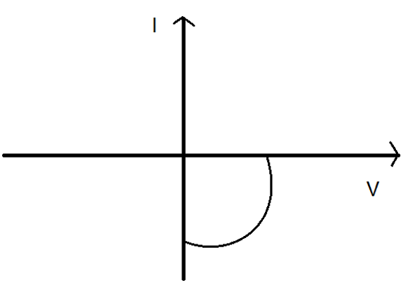
a) Voltage Breakdown
b) RMS Voltage
c) Open Circuit Voltage
d) Short Circuit Voltage
View Answer
Explanation: In the given figure, the point where the graph touches the X-axis shows the open circuit voltage while the point where it touches the Y-axis shows the short circuit current.
7. The I-V characteristics of a solar cell are drawn in the fourth quadrant.
a) True
b) False
View Answer
Explanation: The I-V characteristics of a solar cell is drawn in the fourth quadrant of the coordinate axis because a solar cell does not draw current but supplies the same to the load.
8. What should be the band gap of the semiconductors to be used as solar cell materials?
a) 0.5 eV
b) 1 eV
c) 1.5 eV
d) 1.9 eV
View Answer
Explanation: Semiconductors with band gap close to 1.5 eV are ideal materials for solar cell fabrication. They are made with semiconductors like Si, GaAs, CdTe, etc.
9. Which of the following should not be the characteristic of the solar cell material?
a) High Absorption
b) High Conductivity
c) High Energy Band
d) High Availability
View Answer
Explanation: The Energy Band of the semiconductor should not be too high. It should be around 1.5 eV so that the incident solar radiation can cause the generation of e-h pairs.
10. Which of the following region is coated with a metal?
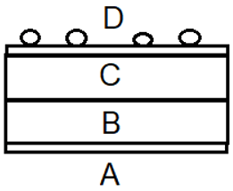
a) A
b) B
c) C
d) D
View Answer
Explanation: In the given figure, A is the back contact which is coated with a metal, B is the p-Si wafer, C is the n-Si wafer and D is the front contact which has metallized finger electrodes.
Sanfoundry Global Education & Learning Series – Engineering Physics.
To practice all areas of Engineering Physics, here is complete set of 1000+ Multiple Choice Questions and Answers.
If you find a mistake in question / option / answer, kindly take a screenshot and email to [email protected]
