This set of Engineering Physics Multiple Choice Questions & Answers (MCQs) focuses on “Classification of Semiconductors”.
1. What is the energy level below which all levels are completely occupied at Zero Kelvin called?
a) Boson Energy
b) Fermi Energy
c) Stable Energy
d) Ground Energy
View Answer
Explanation: Fermi energy is said to be the energy of the highest possible occupied energy level at 0 K. Below this level, all the states are completely occupied.
2. What are the current carriers in semiconductors?
a) Electrons and Protons
b) Electrons and Nucleons
c) Electrons and Photons
d) Electrons and Holes
View Answer
Explanation: Electrons and holes are the two current carriers in semiconductors. Electrons are negatively charged while holes are positively charged. Their movement gives rise to a current in the semiconductor.
3. The concentration of doping is kept below ______________
a) 1 %
b) 5 %
c) 10 %
d) 50 %
View Answer
Explanation: The concentration of doping in semiconductors is generally kept below 1 %. However, it is enough to bring a huge drop in the energy gap.
4. In N-Type semiconductors, which extra energy level is added?
a) Conduction level
b) Donor Energy Level
c) Acceptor energy level
d) Valence level
View Answer
Explanation: In N-Type semiconductor level, a new energy level below the conduction band is formed. The energy difference between the two is about 0.045 eV.
5. Which of the following can be used to create a P-Type Semiconductor?
a) P
b) Sb
c) Ga
d) As
View Answer
Explanation: For a P-Type semiconductor, a material with 3 valence electrons is chosen. Out of the given choices, Ga can be used to create a P-Type Semiconductor.
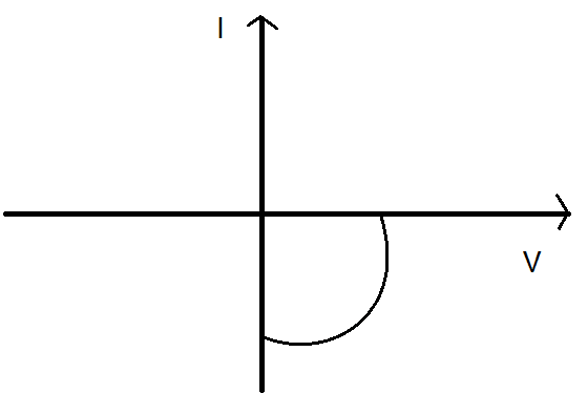
6. The following graph depicts the I-V characteristics of which instrument?
a) Photodiode
b) Light Emitting Diode
c) Solar Cell
d) Zener diode
View Answer
Explanation: The generation of EMF by a solar cell is due to three basic processes: generation of electron-hole pair, separation of electrons and holes and collection of electrons by the front contact.
The p-side becomes positive and the n-side becomes negative giving rise to photo voltage.
The I-V characteristics of the solar cell are drawn in the fourth quadrant of the coordinate axis because a solar cell does not draw current but supplies the same to the load.
7. The Hall coefficient of a specimen is 3.66 x 10⁻⁴ m3C-1. If it’s resistivity is 8.93 x 10⁻³ Ωm, what will be its mobility?
a) 0.01 m2V-1s-1
b) 0.02 m2V-1s-1
c) 0.03 m2V-1s-1
d) 0.04 m2V-1s-1
View Answer
Explanation: We know, Mobility = Hall coefficient/resistivity
Therefore, Mobility = 3.66 x 10⁻⁴/8.93 x 10-3
= 0.04 m2V-1s-1.
8. Which one of the following is not an intrinsic semiconductor?
a) Carbon
b) Silicon
c) Germanium
d) Lead
View Answer
Explanation: There are 4 bonding electrons in all the above materials. However, the energy required to take out an electron will be maximum for carbon as the valence electrons are in the second orbit. Hence, the number of free electrons for conduction is negligibly small in C.
9. Which of the following is n-type semiconductor?
a) CaO
b) MgO
c) ZnO
d) BaO
View Answer
Explanation: II-VI semiconductors are generally p-type semiconductors except for ZnO and ZnTe. II-VI semiconductors are those which contain atoms of materials that have 2 valence electrons and 6 valence electrons.
10. P-Type semiconductor has a lower electrical conductivity than N-Type semiconductor.
a) True
b) False
View Answer
Explanation: Due to comparatively lower mobility of holes than electrons for the same level of doing as in an N-Type semiconductor, it has lower electrical conductivity.
11. Pure Si at 300 K has equal electron (ni) and hole concentration (p) of 1.5 X 10¹⁶ m-3. Doping by indium increases p to 4.5 X 10²² m-3. What is n in the doped silicon?
a) 4.5 X 10⁹ m-3
b) 4.5 X 10²² m-3
c) 5 X 10⁹ m-3
d)5 X 10²² m-3
View Answer
Explanation: Here, ni = 1.5 X 10¹⁶ m-3, p = 4.5 X 10²² m-3
We know, np = ni2
n = ni2/p
= 5 X 10⁹ m-3.
12. Identify the type of material.
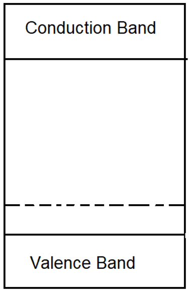
a) Intrinsic Semiconductor
b) N-Type semiconductor
c) P-Type semiconductor
d) Conductor
View Answer
Explanation: In the figure, as we can see there is an acceptor energy level just above the valence band. This happens in the case of P-Type semiconductors.
13. In a semiconductor it is observed that three-quarters of the current is carried by electrons and one quarters by holes. If the drift speed is three times that of the holes, what is the ratio of electrons to holes?
a) 1 : 1
b) 1 : 2
c) 2 : 1
d) 4 : 1
View Answer
Explanation: In a semiconductor, I = Ie + Ih
Here, Ie = 3⁄4 I and Ih = 1⁄4 I
Now ve = 3vh
Ie/Ih = nve/nvh
3 = 3n/p
n = p
Hence the ration is, 1 : 1
14. Holes are the majority carries in Intrinsic Semiconductors.
a) True
b) False
View Answer
Explanation: A pure semiconductor is called an intrinsic semiconductor. Hence, in this case, the number of electrons and holes are same, as the electron that moves out of its position leaves a hole behind. Hence, the concentration of holes and electrons is the same in an intrinsic semiconductor.
15. If the number of electrons (majority carrier) in a semiconductor is 5 X 10²⁰ m-3 and μe is 0.135 mho, find the resistivity of the semiconductor.
a) 0.0926 Ωm
b) 0.0945 Ωm
c) 0.0912 Ωm
d) 0.0978 Ωm
View Answer
Explanation: We know, Conductivity, σ = ene μe
= 5 X 1.6 X 0.135 X 10 mho/m
= 10.8 mho/m
Resistivity = 1/σ
= 0.0926 Ωm.
Sanfoundry Global Education & Learning Series – Engineering Physics.
To practice all areas of Engineering Physics, here is complete set of 1000+ Multiple Choice Questions and Answers.
If you find a mistake in question / option / answer, kindly take a screenshot and email to [email protected]
