This set of Engineering Physics Multiple Choice Questions & Answers (MCQs) focuses on “Characteristics of P-N Junction”.
1. In a P-N Junction, the depletion region is reduced when _________
a) P side is connected to the negative side of the terminal
b) P side is connected to the positive side of the terminal
c) N side is connected to the positive side of the terminal
d) Never reduced
View Answer
Explanation: When the P-side of a P-N junction is connected to the positive terminal of a battery, the junction is forward biased and hence the depletion region reduces.
2. The voltage at which forward bias current increases rapidly is called as ___________
a) Breakdown Voltage
b) Forward Voltage
c) Knee Voltage
d) Voltage barrier
View Answer
Explanation: Till the knee voltage, the current in a semiconductor increases slowly. After Knee voltage, the current increases rapidly for a small change in the voltage.
3. The Knee Voltage for germanium is _________
a) 0.1 V
b) 0.3 V
c) 0.7 V
d) 1.4 V
View Answer
Explanation: Knee voltage or the threshold voltage is the point after which the current increases rapidly. For germanium, it is about 0.3 V while for silicon it is 0.7 V.
4. The resistance of the semiconductor decreases in forward biased.
a) True
b) False
View Answer
Explanation: When a P-N Junction diode is forward biased, the thickness of the depletion region becomes negligibly small. Thus, the resistance of the semiconductor decreases.
5. The current produced in reverse-bias is called as __________
a) Reverse Current
b) Breakdown Current
c) Negative Current
d) Leakage Current
View Answer
Explanation: When the diode is reverse biased, the reverse bias voltage produces an extremely small current, about a few micro amperes. This is called leakage current.
6. Which diode is designed to work under breakdown region?
a) Photodiode
b) Light Emitting Diode
c) Solar Cell
d) Zener diode
View Answer
Explanation: Zener Diode is designed specifically to operate in the breakdown region. It is mostly used as a voltage regulator in various circuits.
7. The P-N junction is a non-ohmic device.
a) True
b) False
View Answer
Explanation: The current-voltage curve of a P-N junction diode is not a straight line. Thus, it does not obey Ohm’s law and is a non-ohmic device.
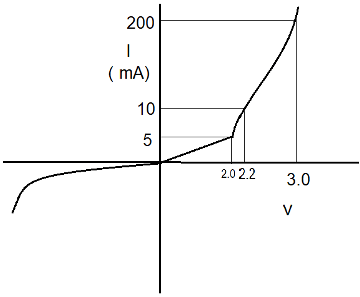
8. The I-V characteristics of a p-n junction diode is shown. What is the resistance of the junction when a forward bias of 2 V is applied?
a) 20 Ω
b) 40 Ω
c) 60 Ω
d) 80 Ω
View Answer
Explanation: The current at 2 V is 5 mA and at 2.2 V it is 10 mA.
The dynamic resistance is: Δ V/Δ I
= 0.5/5 X 103 Ω
= 40 Ω.
9. The leakage current is measured in ________
a) A
b) mA
c) μA
d) nA
View Answer
Explanation: As in the reverse current, the resistance increases, the current produced is extremely low. And hence, it is measured in microamperes.
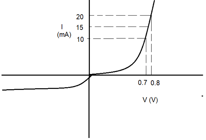
10. From the I-V characteristics, calculate the resistance of the diode at I = 15 mA.
a) 10 Ω
b) 12 Ω
c) 14 Ω
d) 15 Ω
View Answer
Explanation: From the curve, I = 20 mA, V = 0.8 V, I = 10 mA when V = 0.7 V
Now, R = Δ V/Δ I
= 0.1 V/10 mA
= 10 Ω.
Sanfoundry Global Education & Learning Series – Engineering Physics.
To practice all areas of Engineering Physics, here is complete set of 1000+ Multiple Choice Questions and Answers.
If you find a mistake in question / option / answer, kindly take a screenshot and email to [email protected]
