This set of VLSI Multiple Choice Questions & Answers (MCQs) focuses on “nMOS and CMOS Fabrication”.
1. What is Lithography?
a) Process used to transfer a pattern to a layer on the chip
b) Process used to develop an oxidation layer on the chip
c) Process used to develop a metal layer on the chip
d) Process used to produce the chip
View Answer
Explanation: Lithography is the process used to develop a pattern to a layer on the chip.
2. Silicon oxide is patterned on a substrate using ____________
a) Physical lithography
b) Photolithography
c) Chemical lithography
d) Mechanical lithography
View Answer
Explanation: Silicon oxide is patterned on a substrate using Photolithography.
3. Positive photo resists are used more than negative photo resists because ___________
a) Negative photo resists are more sensitive to light, but their photo lithographic resolution is not as high as that of the positive photo resists
b) Positive photo resists are more sensitive to light, but their photo lithographic resolution is not as high as that of the negative photo resists
c) Negative photo resists are less sensitive to light
d) Positive photo resists are less sensitive to light
View Answer
Explanation: Negative photo resists are more sensitive to light, but their photo lithographic resolution is not as high as that of the positive photo resists. Therefore, negative photo resists are-used less commonly in the manufacturing of high-density integrated circuits.
4. The ______ is used to reduce the resistivity of poly silicon.
a) Photo resist
b) Etching
c) Doping impurities
d) None of the mentioned
View Answer
Explanation: The resistivity of poly silicon is reduced by Doping impurities.
5. The isolated active areas are created by technique known as ___________
a) Etched field-oxide isolation
b) Local Oxidation of Silicon
c) Etched field-oxide isolation or Local Oxidation of Silicon
d) None of the mentioned
View Answer
Explanation: To create isolated active areas both the techniques can be used. Among them Local Oxidation of Silicon(LOCOS) is most efficient.
6. The chemical used for shielding the active areas to achieve selective oxide growth is?
a) Silver Nitride
b) Silicon Nitride
c) Hydrofluoric acid
d) Polysilicon
View Answer
Explanation: Selective oxide growth is achieved by shielding the active areas. Silicon nitride (Si3N4) is used for shielding the active areas during oxidation, which effectively inhibits oxide growth.
7. The dopants are introduced in the active areas of silicon by using which process?
a) Diffusion process
b) Ion Implantation process
c) Chemical Vapour Deposition
d) Either Diffusion or Ion Implantation Process
View Answer
Explanation: Two ways to add dopants are diffusion and ion implantation.
8. To grow the polysilicon gate layer, which of the following chemical is used for chemical vapour deposition?
a) Silicon Nitride(Si3N4)
b) Silane gas(SiH4)
c) Silicon oxide
d) None of the mentioned
View Answer
Explanation: Silicon Wafer is placed in a reactor with silane gas (SiH4), and they are heated again to grow the polysilicon layer by chemical vapor deposition.
9. The process by which Aluminium is grown over the entire wafer, also filling the contact cuts is?
a) Sputtering
b) Chemical vapour deposition
c) Epitaxial growth
d) Ion Implantation
View Answer
Explanation: Aluminum is sputtered over the entire wafer, it also fills the contact cuts.
10. Which process is involved in growing the shaded region?
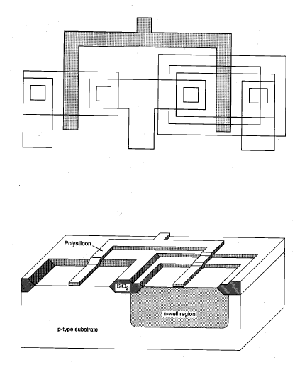
a) Chemical vapor deposition (CVD)
b) Sputtering and patterned by etching
c) Chemical vapor deposition (CVD) and patterned by HF acid etching
d) Chemical vapor deposition (CVD) and patterned by dry (plasma) etching
View Answer
Explanation: The poly silicon layer is produced using chemical vapor deposition (CVD) and it is patterned by dry (plasma) etching.
11. Chemical Mechanical Polishing is used to ___________
a) Remove silicon oxide
b) Remove silicon nitride and pad oxide
c) Remove polysilicon gate layer
d) Reduce the size of the layout
View Answer
Explanation: The pad oxide and nitride are removed using a Chemical Mechanical Polishing (CMP) step.
12. Gate oxide layer consists of ___________
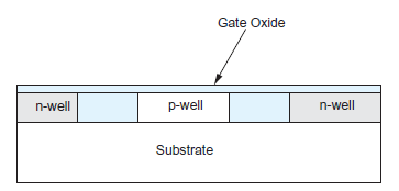
a) SiO2 layer, overlaid with a few layers of an oxynitrided oxide
b) Only SiO2 Layer
c) SiO2 layer with Polysilicon Layer
d) SiO2 layer and stack of epitaxial layers of Polysilicon
View Answer
Explanation: Current processes seldom use a pure SiO2 gate oxide, but prefer to produce a stack that consists of a few atomic layers, each 3–4 Å thick, of SiO2 for reliability, overlaid with a few layers of oxy-nitrided oxide (one with nitrogen added).
13. What is Piranha Solution?
a) It is a 3:1 to 5:1 mix of nitric acid and hydrogen peroxide that is used to develop the oxide layer on silicon substrate
b) It is a 3:1 to 5:1 mix of sulphuric acid and hydrofluoric acid that is used to clean silicon wafers removing organic and metal contaminants or photo resist after metal patterning
c) It is a 3:1 to 5:1 mix of sulphuric acid and hydrogen peroxide that is used to grow the oxide layer on the silicon
d) It is a 3:1 to 5:1 mix of sulphuric acid and hydrogen peroxide that is used to clean wafers of organic and metal contaminants or photo resist after metal patterning
View Answer
Explanation: Piranha solution is a 3:1 to 5:1 mix of sulfuric acid and hydrogen peroxide that is used to clean silicon wafers of metal and organic contaminants or photo-resist after metal patterning.
Sanfoundry Global Education & Learning Series – VLSI.
To practice all areas of VLSI, here is complete set of 1000+ Multiple Choice Questions and Answers.
If you find a mistake in question / option / answer, kindly take a screenshot and email to [email protected]
