This set of VLSI Multiple Choice Questions & Answers (MCQs) focuses on “Capacitive Loads and Wiring Capacitances”.
1. The capacitances in MOSFET occurs due to _____________
a) Interconnects
b) Difference in Doping concentration
c) Difference in dopant materials
d) All of the mentioned
View Answer
Explanation: The on-chip capacitances found in MOS circuits are due to interconnects, difference in Doping concentration, difference in dopant materials.
2. The parasitic capacitances found in MOSFET are ___________
a) Oxide related capacitances
b) Inter electrode capacitance
c) Electrolytic capacitance
d) All of the mentioned
View Answer
Explanation: The parasitic device capacitances can be classified into two major groups: oxide-related
capacitances and junction capacitances.
3. The proper DC model of MOSFET with capacitances is?
a) 
b) 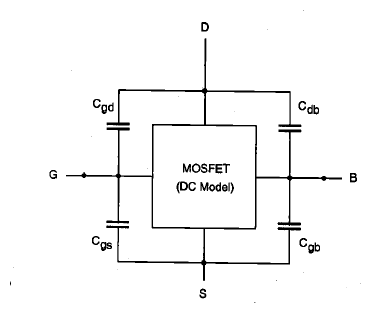
c) 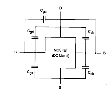
d) None of the mentioned
View Answer
Explanation: The capacitances exist between all the regions of the MOSFET.
4. The capacitance that exist between Gate and Bulk is called as ___________
a) Oxide parasitic capacitance
b) Metal oxide capacitance
c) MOS capacitance
d) None of the mentioned
View Answer
Explanation: The capacitance that exist between Gate and Bulk is called as an oxide parasitic capacitance.
5. In Cut-off Mode, the capacitance Cgs will be equal to ___________
a) 2Cgd
b) 0
c) Cgb
d) All of the mentioned
View Answer
Explanation: In cut-off mode, the conducting channel does not exist, so gate-to-source and the gate-to-drain capacitances are both equal to zero.
6. In cut-off mode, the value of gate to substrate capacitance is equal to ___________
a) Cox .(W- L)
b) Cox W/ L
c) Cox* W*L
d) 0
View Answer
Explanation: In Cut-off mode, the conducting channel does not exist, so gate-to-source and the gate-to-drain capacitances are both equal to zero. Therefore, the gate to substrate capacitance is equal to Cox* W*L.
7. In linear mode operation, the parasitic capacitances that exists are ___________
a) Nonzero Gate to source capacitance
b) Nonzero Gate to drain capacitance
c) Zero gate to substrate capacitance
d) All of the mentioned
View Answer
Explanation: In linear-mode operation, the conducting channel exists, therefore there will be a finite amount of gate to source and gate to drain capacitances. Since the conducting channel exists, gate to substrate capacitance is reduced to zero.
8. In saturation mode operation, gate to drain capacitance is zero due to ___________
a) Gate and drain are interconnected
b) Channel length is reduced
c) Inversion layer doesn’t exist
d) Drain is connected to ground
View Answer
Explanation: Due to the pinched off channel, the capacitance between source to drain is reduced to zero.
9. When MOSFET is operating in saturation region, the gate to source capacitance is?
a) 1/2*Cox*W*L
b) 2/3*Cox*W*L
c) Cox*W*L
d) 1/3*Cox*W*L
View Answer
Explanation: Due to the reduction in channel length, gate to drain and gate to substrate capacitance are zero, the gate to channel capacitance as seen between the gate and the source is approximately defined as 2/3*Cox*W*L.
10. In the below graph, the regions marked as A,B,C are?
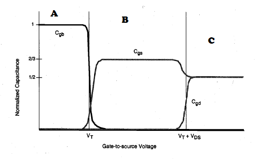
a) A : Saturation, B : Linear, C : Cut-off
b) A : Cut-off, B : Linear, C : Saturation
c) A : Linear, B : Saturation, C : Cut-off
d) None of the mentioned
View Answer
Explanation: The gate to substrate capacitance exists only in cut-off region, and gate to drain capacitance exist only in saturation region.
Hint: the graph can be analyzed from the gate to source voltage on x axis and regions can be determined.
11. The load capacitance is measured between ___________
a) Output node and input node
b) Output node and Vcc
c) Output node and ground
d) Input node and ground
View Answer
Explanation: The load capacitance is measured at output node and ground.
12. The load capacitance is equivalent to ___________
a) Sum of all lumped linear capacitances between input and output node
b) Sum of all junction capacitance between Vcc and ground
c) Sum of all junction capacitance between input and output
d) Sum of all lumped linear capacitances between output node and ground
View Answer
Explanation: The load capacitance is measured by sum of all lumped linear capacitances between input and output node.
13. Interconnect capacitance contributes to the load capacitance when the CMOS inverters are connected in cascade configuration.
a) True
b) False
View Answer
Explanation: In cascade configuration the load capacitance is measured by sum of all the lumped capacitances and interconnect capacitance.
14. Interconnect capacitance is formed due to ___________
a) Junction capacitance between gate and substrate
b) Wire connecting the gates of 2 different inverters
c) Parasitic capacitance existing between metal and polysilicon connection between 2 inverters
d) All of the mentioned
View Answer
Explanation: Parasitic capacitance existing between metal and polysilicon connection between 2 inverters causes the interconnect capacitance.
15. Which of the following parameters are found using load capacitance?
a) Delay time
b) Power consumption
c) Speed of the CMOS logic
d) All of the mentioned
View Answer
Explanation: Using load capacitance, delay time, power consumption, speed of the CMOS logic can be measured.
Sanfoundry Global Education & Learning Series – VLSI.
To practice all areas of VLSI, here is complete set of 1000+ Multiple Choice Questions and Answers.
If you find a mistake in question / option / answer, kindly take a screenshot and email to [email protected]
