This set of VLSI Multiple Choice Questions & Answers (MCQs) focuses on “CMOS Logic Gates”.
1. In negative logic convention, the Boolean Logic [1] is equivalent to:
a) +VDD
b) 0 V
c) -VDD
d) None of the mentioned
View Answer
Explanation: In negative logic convention, the Boolean Logic [1] is equivalent to 0 V and Logic ‘0’ is equivalent to +VDD.
2. In positive logic convention, the true state is represented as:
a) 1
b) 0
c) -1
d) -0
View Answer
Explanation: In positive logic convention, the Boolean logic ‘1’ is known to be representing true state.
3. The CMOS gate circuit of NOT gate is:
a) 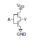
b) 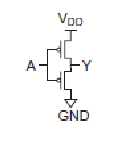
c) 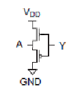
d) 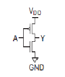
View Answer
Explanation: The CMOS logic circuit for NOT gate has a p-MOS as a pull up transistor and n-MOS as driver transistor which is represented accurately in the below figure
4. The truth table which accurately explains the operation of CMOS not gate is:
a) 
b) 
c) 
d) 
View Answer
Explanation: The output of CMOS depends on the state of nMOS and pMOS transistor.The correct truth table is:
5. The CMOS logic circuit for NAND gate is:
a) 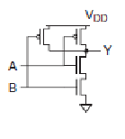
b) 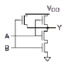
c) 
d) None of the mentioned
View Answer
Explanation: The accurate cmos logic circuit for NAND gate is:
6. In CMOS logic circuit the n-MOS transistor acts as:
a) Load
b) Pull up network
c) Pull down network
d) Not used in CMOS circuits
View Answer
Explanation: A static CMOS gate has an nMOS pull-down network to connect the output to 0 (GND).
7. In CMOS logic circuit the p-MOS transistor acts as:
a) Pull down network
b) Pull up network
c) Load
d) Short to ground
View Answer
Explanation: A static CMOS gate has a pMOS pull-up network to connect the output to VDD (1).
8. In CMOS logic circuit, the switching operation occurs because:
a) Both n-MOSFET and p-MOSFET turns OFF simultaneously for input ‘0’ and turns ON simultaneously for input ‘1’
b) Both n-MOSFET and p-MOSFET turns ON simultaneously for input ‘0’ and turns OFF simultaneously for input ‘1’
c) N-MOSFET transistor turns ON, and p-MOSFET transistor turns OFF for input ‘1’ and N-MOS transistor turns OFF, and p-MOS transistor turns ON for input ‘0’
d) None of the mentioned
View Answer
Explanation: In CMOS logic circuit, the switching operation occurs because N-MOS transistor turns ON, and p-MOS transistor turns OFF for input ‘1’ and N-MOS transistor turns OFF, and p-MOS transistor turns ON for input ‘0’. The networks are arranged such that one is ON and the other OFF for any input pattern.
9. The CMOS logic circuit for NOR gate is:
a) 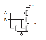
b) 
c) 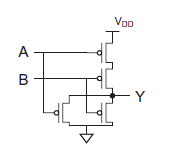
d) 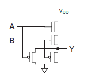
View Answer
Explanation:
10. When both nMOS and pMOS transistors of CMOS logic design are in OFF condition, the output is:
a) 1 or Vdd or HIGH state
b) 0 or ground or LOW state
c) High impedance or floating(Z)
d) None of the mentioned
View Answer
Explanation: When both pull up and pull down transistors are OFF, the high impedance for floating Z output state results.
11. When both nMOS and pMOS transistors of CMOS logic gates are ON, the output is:
a) 1 or Vdd or HIGH state
b) 0 or ground or LOW state
c) Crowbarred or Contention(X)
d) None of the mentioned
View Answer
Explanation: The crowbarred (or contention) X level exists when both pull up and pull down transistors are simultaneously turned ON. Contention between the two networks results in an indeterminate output level and dissipates static power.
Sanfoundry Global Education & Learning Series – VLSI.
To practice all areas of VLSI, here is complete set of 1000+ Multiple Choice Questions and Answers.
If you find a mistake in question / option / answer, kindly take a screenshot and email to [email protected]
