This set of Linear Integrated Circuit Multiple Choice Questions & Answers (MCQs) focuses on “Band-Reject and All-Pass Filters”.
1. How many types of band elimination filters are present
a) Three
b) Two
c) Four
d) None of the mentioned
View Answer
Explanation: Band-reject filters are also called as band elimination filters. They are classified into two types.
i) Wide band-reject filter and
ii) Narrow band-reject filter.
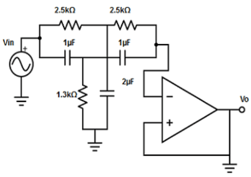
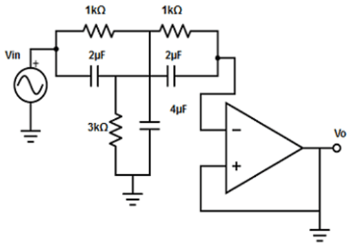
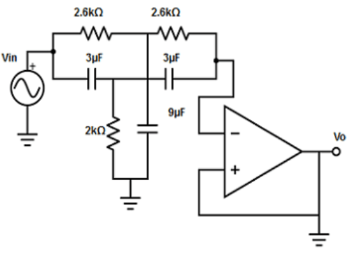
2. Find the wide band-reject filter.
a)
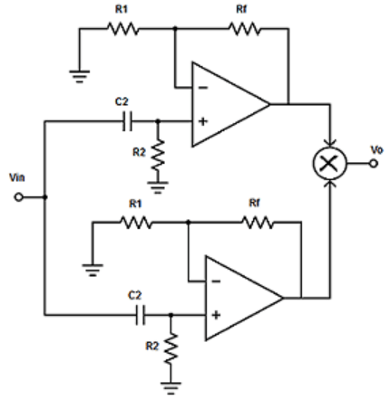
b)
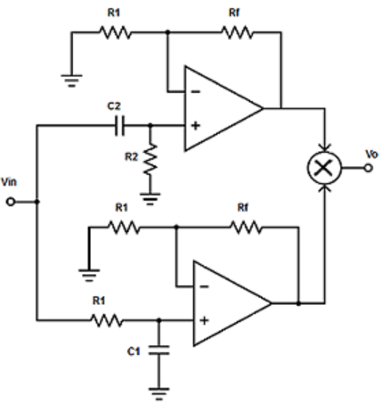
c)
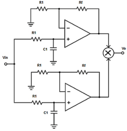
d) None of the mentioned
View Answer
Explanation: A wide band-reject filter is made using a low pass filter, a high pass filter and a summing amplifier.
3. A narrow band-reject filter is commonly called as
a) Notch filter
b) Band step filter
c) Delay filter
d) All of the mentioned
View Answer
Explanation: A narrow band-reject filter is also called as notch filter because of its higher quality factor, Q (>10).
4. Find the expression for notch-out frequency?
a) fN = 2πRC
b) fN = 2π/RC
c) fN = 1/2π×√(R/C)
d) fN = 1/2πRC
View Answer
Explanation: The notch-out frequency is the frequency at which maximum attenuation occurs: it is given by fN =1/2πRC.
5. The quality factor of passive twin T-network is increased by using
a) Inverting amplifier
b) Non-inverting amplifier
c) Voltage follower
d) Differential amplifier
View Answer
Explanation: The passive twin T-network has a selectively low figure of merit. The Q of the network can be increased significantly, if it is used with the voltage follower.
6. Find out the application in which narrow band-reject filter can be used?
a) Embedded system
b) Biomedical instrument
c) Digital computer
d) None of the mentioned
View Answer
Explanation: Notch filters or narrow band-reject filters are used in biomedical instruments for eliminating undesired frequencies.
7. Design 120Hzactive notch filter?
a)
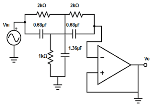
b)
c)
d)
View Answer
Explanation: Since C value < 0.1µF, assume C=0.68µF Notch Frequency, fn = 1/2πRC.
R= 1/(2πfnC)= 1/(2π×120Hz×0.68×10-6) = 1.95kΩ ≅2kΩ.
For R/2, parallel of two 2kΩ resistor
=>R/2 = 2kΩ||2kΩ =(2×2)/(2+2)=1kΩ.
For C/2 , parallel of two 0.68µF capacitor
C/2=> 0.68µF + 0.68µF= 1.36µF.
8. Find the application of area where all-pass filters are used?
a) Cathode ray oscilloscope
b) Television
c) Telephone wire
d) None of the mentioned
View Answer
Explanation: When signals are transmitted in transmission lines like telephone wire, they undergo change in phase, all-pass filters are used to compensate these phase changes.
9. Determine the output voltage for all the all-pass filter and express it in complex form?
a) VO =Vin/ [(1-j2πfRC) /(1+ j2πfRC)].
b) VO =Vin× [(1+j2πfRC) /(1- j2πfRC)].
c) VO =Vin ×[(1- j2πfRC) /(1+ j2πfRC)].
d) None of the mentioned
View Answer
Explanation: The output voltage of all-pass filter is given as VO =Vin× [(1-j2πfRC) /(1+j2πfRC)] .
10. Determine the input frequency for all-pass filter with phase angle as 62o. Consider the value of resistor and capacitor are 3.3kΩ and 4.7µF.
a) Input frequency= -7.65Hz
b) Input frequency= -6.77Hz
c) Input frequency= -3.89Hz
d) Input frequency= -9.65Hz
View Answer
Explanation: The phase angle is given as Φ = -2tan-1×(2πfRC)
=> f=-tanΦ/4πRC =-tan(62o)/(4π×3.3kΩ×4.7µF)= -1.88/0.1948 =-9.65Hz.
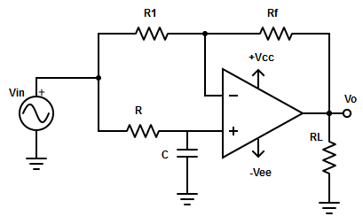
11. Determine the angle for given circuit diagram, if the frequency of input signal is 1khz
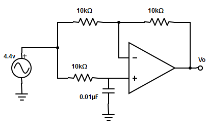
a) -45o
b) -180o
c) -270o
d) -90o
View Answer
Explanation: Phase angle Φ=-2tan-1×(2πfRC/1) = -2tan-1×(2π×1kHz×16kΩ×0.01µF)
= -2tan-1×(1.0048)=-90o.
12. The voltage gain magnitude of all-pass filter is
a) Zero
b) One
c) Infinity
d) None of the mentioned
View Answer
Explanation: The magnitude of voltage gain of all-pass filter |VO /Vin| = √(1+(2π/RC)2) / √(1+(2 π/RC)2) =1.
13. What happens if the position of R and C are interchanged in the below circuit diagram?
a) Vin leads VO
b) Vin lags VO
c) VO leads Vin
d) VO leads Vin
View Answer
Explanation: For the circuit given, the phase angle changes from 0 to 180o as frequency is varied from 0 to ∞. If the positions of R and C are interchanged, the phase shift and band width input and output becomes positive. That is the output (VO) leads input (Vin).
14. Choose the incorrect statement “In wide band-reject filter” .
a) Low cut-off frequency of low pass filter must be larger than the high cut-off frequency of the high pass filter.
b) Low cut-off frequency of high pass filter must be equal than the high cut-off frequency of the high pass filter.
c) Low cut-off frequency of high pass filter must be smaller than the high cut-off frequency of the low pass filter.
d) None of the mentioned
View Answer
Explanation: In wide band-reject filter, low cut-off frequency of high pass filter must be larger than the high cut-off frequency of the low pass filter.
Sanfoundry Global Education & Learning Series – Linear Integrated Circuits.
To practice all areas of Linear Integrated Circuits, here is complete set of 1000+ Multiple Choice Questions and Answers.
If you find a mistake in question / option / answer, kindly take a screenshot and email to [email protected]
